Two-dimensional crystals feel the pressure
Two-dimensional (2D) crystals can be attained by exfoliation of van der Waals materials. The latter are formed by atomic layers held together by weak electrostatic forces, akin to graphene in graphite. Since the discovery of graphene twenty years ago, the number of 2D crystals has increased enormously, encompassing materials with metallic, insulating and semiconducting properties.
Semiconducting 2D crystals are particularly ripe with novel physical phenomena and great applicative prospects. Certainly, the success of a material system hinges on our capability to engineer its physical properties. In this respect, 2D materials and the corresponding physical properties can be widely modulated through various approaches that act directly on the band structure of the lattice, such as hetero-structuring, doping, alloying, the creation of defects, the application of electromagnetic fields, or mechanical deformations. Mechanical deformations rely on a change of the lattice structure by strain engineering (i.e., by stretching or compressing the crystal plane controllably) or by hydrostatic pressure. Indeed, mechanical tuning methods are uniquely efficacious in 2D semiconductors thanks to their all-surface nature and ensuing much stronger deformation capacity compared to covalently bound bulk lattices.
In a work published in Nano Letters [1], three young scientists of our Department, Elena Stellino and Beatrice D’Alò (at the HPS group) and Elena Blundo (at the OPERA group ), show that external hydrostatic pressure and morphological strain can be efficiently combined in transition metal dichalcogenide (TMD, such as MoS2 and WS2) 2D semiconductors.That approach, which represents a remarkable experimental challenge, has been rarely used despite its extremely insightful nature.
First, morphological strain was achieved by hydrogen irradiation of bulk WS2 that leads to the formation of hydrogen-filled, micrometer-sized, spherical bubbles made of a monolayer directly lifted from the underlying bulk lattice [2]. Owing to the membrane curvature and hydrogen internal pressure of tens to hundreds of atm, the monolayer experiences a biaxial tensile strain at the dome center (resulting in a record total strain of about 4%).
Through a painstaking exfoliation and deposition procedure, the authors succeeded to place WS2 bubbles between the culets of a diamond anvil cell.
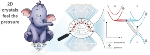
Secondly, exploiting the enormous force exerted by the diamond anvil cell culets, the authors applied a pressure in excess of 6000 atm on a monolayer bubble of WS2.That pressure corresponds to the pressure which would be applied by an adult elephant sitting on a 1 cm2 surface. Remarkably, the bubble withstood such a huge pressure and the modification of the crystal shape permitted a controlled modulation of the strain gradients at work on the system. By combining the results from micro-Raman and micro-photoluminescence experiments, the authors unveiled an anomalous pressure evolution of the band extremes in the conduction band (CB), responsible for the pronounced non-linearity observed in both the intensity and energy trend of the exciton band under pressure. A hybridization mechanism between distinct CB extremes was proposed. The crossover between different CB minima and their hybridization occurs at pressure values much lower than those predicted for planar monolayers, resulting in an exciton emission with a mixed direct/indirect nature and in-plane/out-of-plane orbital character.
The work frames a complete scenario for the pressure response of 2D crystals, which includes the evolution of their morphological features, lattice properties and electronic band structure and thus defines a new approach to investigate and, possibly, engineer the optoelectronic properties of 2D materials with prospects for pressure sensors.
[1] Elena Stellino, Beatrice D'Alò, Elena Blundo, Paolo Postorino, and A. Polimeni, Nano Lett. 2024; ACS Publications
[2] E. Blundo et al., Phys. Rev. Lett. 127, 046101 (2021)